


 English
 Chinese


Search
Buyers Here
Suppliers Here
 Select Language
Products Suppliers
Recent Searches Clear
History
 All Categories
 Home
Thick/Heavy Copper PCB
Home
Thick/Heavy Copper PCB
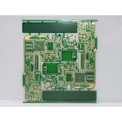


Thick/Heavy Copper PCB
Min. Order: 1
Payment: cash
Minimum Order: -
Delivery: 4-7days
Origin: china
Packing: -
Inspection: -
Sample Price: $50.00


Product Attributes
Company Profile
Logistics and other information
Product Details
Thick Copper PCB Difinition and Thickness
There is no exact definition of thick copper in the PCB industry. Generally, the copper thickness ≥ 2oz is defined as Heavy copper PCB. Heavy copper PCB is mainly used in high-current electronic products. High-current electronic products are generally high-power or high-voltage PCBs. They are mostly used in automotive electronics, communication equipment, aerospace, planar transformers, and secondary power modules.
Our thickest copper PCB can make 6 ounces. However, considering the side eclipse factor, copper thickness of more than 3 ounces should pay special attention to the line width of the inner layer.
Inner 3 oz copper pcb: line width 6/7 mil outer 3 ounces: line width 8/12 mil
Inner layer 4 oz copper pcb: line width line spacing 8/11 mil outer layer 3 ounces: line width line spacing 9/15 mil
Inner 5 oz copper pcb: line width 10/16 mil outer 3 ounces: line width 11/16 mil
Inner 6 oz copper pcb: line width line spacing 12/18 mil outer layer 3 ounces: line width line spacing 14/18 mil
Heavy Copper PCB Production Difficulties
1. If the etching is not clean during the etching process, the pressure will not reach the standard, and if it is serious, it will cause the line to short-circuit.
2. Heavy Copper PCB dense lines are prone to foaming during solder mask ink fabrication
3. Heavy Copper PCB has the highest scrap rate in the inner layer of the drilling process, the hole is thick, the nail head is the highest.
4. In the pressing process, it is easy to have insufficient glue filling, excessive flow glue, uneven thickness, void and so on.
When the electronic device need high power or current through, Then we need consider heave copper to control the thermal on PCB, Thermal management is more important than ever today as electronics are used in demanding environments and Operative at higher currents. Heavy copper PCBs (copper conductors 5 oz/ft2 – 19 oz/ft2 in inner And/or outer layers; sometimes defined as more than 4 oz per square foot (ft2)) can help conduct heat away from components so failure is greatly reduced. PCB manufacturers create durable wiring platforms with heavy copper. And boards may be manufactured in a smaller footprint as they can contain multiple weights of copper on the same circuit layers.
The Benefits of Heavy Copper PCBs include: Reduction of Thermal Strain
A. Better current conductivity
B. Can travelers repeated thermal cycling
C. Smaller PCB size due to layering of copper
D. Increased connector site strength
Welcome to custom Thick Copper PCB Board directly from Heavy Copper PCB Manufacturer at low cost.
Related Keywords
manufacturer
factory
supplier
export
price
Industrial
Power
Supply
Our Products Range
Inquiry Basket ( 0 ) Send Inquiry
Contact Supplier
( 0 )
No information
Contact Supplier
Send Inquiry